
TDI Cameras for Semiconductor Metrology & Inspection
TDI Cameras for Semiconductor Metrology & Inspection
1. What is TDI
A TDI Camera (Time Delay Integration Camera) is a high-performance line scan camera designed exclusively for imaging fast-moving objects. With its unique synchronous charge transfer mechanism, it delivers high-SNR, high-resolution clear images under extremely low light conditions, widely deployed in industrial inspection, remote sensing, semiconductors, biomedical imaging, national defense and other fields.
TDI imaging is suitable for recording linear processes that change over time, or scenarios with highly asymmetric aspect ratios of target objects. TDI technology excels in low-light scanning applications where standard line scan cameras fail to produce usable images.
2. Working Principle of TDI
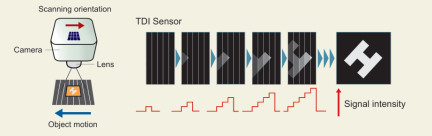
Time Delay Integration is a scanning technology that uses stacked linear pixel arrays aligned and synchronized with the movement direction of the target object to generate continuous 2D images of moving targets. As the image projection shifts from one pixel row to the next, accumulated charges shift synchronously, enabling higher resolution imaging under lower illumination than standard line scan cameras.
In FFT-CCD sensors, signal charges on each row shift vertically during readout. TDI mode synchronizes this vertical charge transfer timing with object motion, so the number of charge integration cycles equals the number of vertical CCD pixel stages. In TDI operation, signal charges must travel at the same speed and direction as the moving target. The speed correlation formula is shown below:
v: Object movement speed / Charge transfer speed; f: Vertical transfer frequency; d: Pixel size
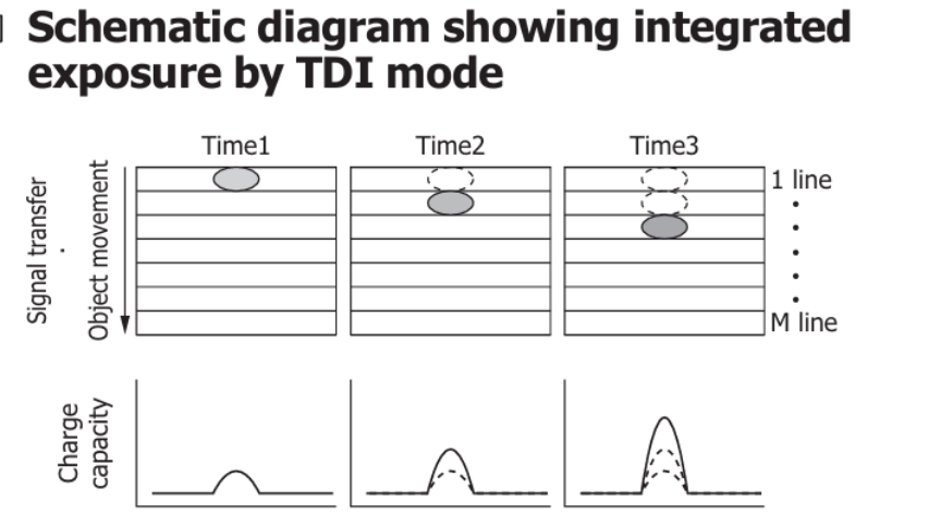
The diagram below intuitively illustrates the imaging effect of cumulative charge integration.
3. Key Industrial Applications of TDI Cameras
1. Wafer Defect Inspection
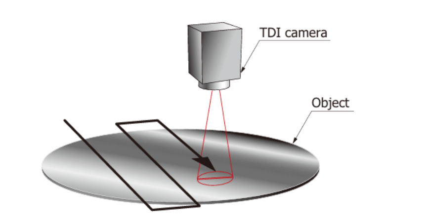
Tiny surface defects on wafers can cause complete chip failure during semiconductor manufacturing. TDI cameras perform inline full-surface scanning of wafers to capture and locate micro defects. Thanks to their high SNR output under low light, TDI systems reliably detect subtle scratches, particle contamination and material inhomogeneity.
2. Photomask Inspection
Photomasks are templates used to transfer circuit patterns onto silicon wafers. Any flaw on a photomask will be replicated onto mass-produced wafers and lead to production scrap. TDI cameras deliver ultra-precise photomask inspection to eliminate defects and guarantee high-quality semiconductor production.
3. Wafer Alignment & Dimensional Metrology
Precise alignment is a critical step in semiconductor fabrication. TDI cameras support high-precision inter-wafer alignment and dimensional measurement, enabling advanced packaging technologies such as 3D stacked chips, which improves chip performance and reliability.
4. Microstructure Analysis
As semiconductor device feature sizes keep shrinking, high-resolution microstructure analysis becomes increasingly vital. TDI cameras offer superior spatial resolution and sensitivity to capture nanoscale surface details, supporting R&D of new semiconductor materials and processes.
TDI cameras support ultra-high line rates, making them ideal for semiconductor metrology scenarios.
4. Leading TDI Camera Manufacturers
Only a handful of manufacturers develop high-end TDI cameras. For products with bandwidth ≥100Gbps, domestic Chinese suppliers hold global leading technical advantages based on public application data.
- BRIGATES (Ruixin Micro) LCG-M2K15CF1-L3P0M-1016 High-speed TDI linear array camera: The 3M line rate 100Gbps model has been mass-delivered to top metrology manufacturers. 200Gbps and 300Gbps versions are scheduled for launch in 2027. Equipped with self-developed image sensors, with maximum technical potential.
- Tucsen (Tusen Optics) Gemini 8KTDI 8K High-Speed TDI Line Scan Camera: The 8K 1MHz line rate 100Gbps product is mass-supplied to leading semiconductor inspection clients. Adopts Gpixel sensors and holds early market entry advantages.
- Gpixel (Changguang Chenxin): 100Gbps TDI cameras are currently under customer sampling, with mass production scheduled for late 2026.
5. Solutions Provided by StarTest Electronics
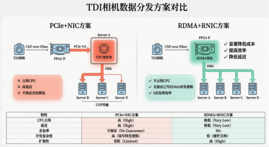
StarTest Electronics’ PCIe-3004 4-Channel CoaXPress Over Fiber Frame Grabber delivers full protocol and hardware support for 100Gbps high-bandwidth data transmission. The company also provides customized acquisition hardware services for semiconductor customers to reduce total costs, boost data processing throughput and minimize transmission latency.
PCIe-3004 4-Channel 25G Fiber CoaXPress Frame Grabber - Chongqing StarTest Electronics Co., Ltd.
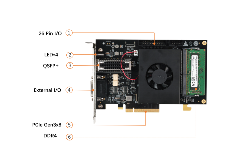
Traditional frame grabber deployment requires multiple servers paired with high-bandwidth RDMA networks or extra frame grabbers for data forwarding, relying on parallel computing across dozens of servers. StarTest Electronics provides FPGA embedded data processing and RDMA data distribution platforms, which drastically cut hardware costs, improve processing efficiency and lower end-to-end latency.